What We Have Covered in This Article
Last Updated on April 9, 2023 by Editor Futurescope
As a chip maker, I often get asked about the process of lithography and its role in the production of semiconductors. Lithography is a crucial step in chip manufacturing that involves transferring a pattern from a photomask to a substrate. This process is primarily done using steppers and scanners that are equipped with optical light sources.
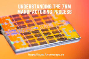
During lithography, the chip wafer is inserted into a lithography machine where it is exposed to deep ultraviolet (DUV) or extreme ultraviolet (EUV) light. This determines just how small the transistors on a chip can be. The lithography process enables the creation of the all-important transistors, which are one of the basic building blocks of modern electronics.
The technology of projecting a pattern onto a material as an outline for the next manufacturing step is known as lithography. For semiconductor chips, a huge drawing of a single chip at its various stages is reduced in size to fractions of an inch and repeated over the size of the chip wafer. The process also includes direct-write e-beam and nanoimprint lithography, among other forms of lithography.
History of Lithography in Chip Making
I find it fascinating to learn about the history of lithography, which has been an essential process in the manufacture of computer chips since its inception. In the 1950s, when the first integrated circuits were being developed, photolithography was used to transfer patterns onto silicon wafers. Back then, the technology was relatively simple, and the patterns were created using contact printing. Over the years, lithography has evolved significantly, and the industry has moved from contact printing to proximity printing and then to projection printing. The introduction of projection printing in the 1980s allowed for the printing of smaller features and paved the way for the development of microprocessors. As the demand for smaller and more complex chips increased, the industry had to find ways to print smaller features. The introduction of deep ultraviolet lithography in the 1990s allowed for the printing of features as small as 0.18 microns.
However, as the industry continued to push the boundaries of what was possible, it became clear that new technologies were needed to print even smaller features. Today, the industry is using extreme ultraviolet (EUV) lithography to print features as small as 7 nanometers. EUV lithography uses a 13.5 nm wavelength, which is much smaller than the 193 nm wavelength used in deep ultraviolet lithography. This technology has allowed for the development of advanced chips that are faster, more powerful, and more energy-efficient than ever before. In conclusion, the history of lithography in chip making is a story of innovation and progress. From the early days of contact printing to the cutting-edge technology of EUV lithography, the industry has continued to push the boundaries of what is possible. As a result, we now have access to some of the most advanced and powerful computer chips ever created.
The Lithography Process for Chip Making
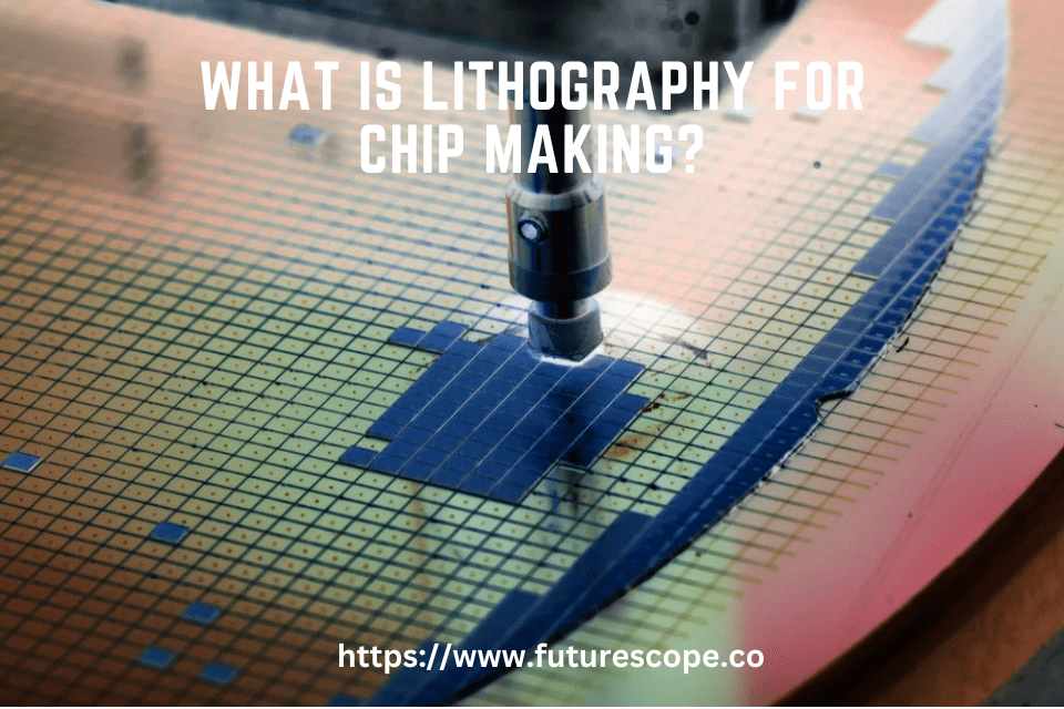
During the chip making process, lithography is a crucial step that determines how small the transistors on a chip can be. In this process, the chip wafer is inserted into a lithography machine where it is exposed to deep ultraviolet (DUV) or extreme ultraviolet (EUV) light. The lithography process can be compared to a slide projector. The light passes through a photomask on which the blueprint or template is located, and instead of being enlarged in size, it is reduced. The structures are then imaged on the wafer that has been coated with a light-sensitive photoresist film. There are different types of lithography processes, including optical lithography, electron beam lithography, and X-ray lithography.
However, the most commonly used process in the semiconductor industry is optical lithography, which uses light to transfer the pattern onto the wafer. The lithography machines used in chip making are highly sophisticated and require extreme precision. The machines must be able to align the wafer to the photomask accurately and expose the photoresist film with the correct amount of light. The lithography process is also a critical factor in determining the cost of chip production, as it requires expensive equipment and materials. In recent years, chip manufacturers have been using EUV lithography, which uses a shorter wavelength of light to achieve higher resolution and smaller feature sizes. However, this process is still relatively new and requires significant investment in equipment and infrastructure.
Types of Lithography Used in Chip Making
In order to create the complex patterns and features required in modern semiconductor chips, different types of lithography systems are used for different layers. Here are some of the most common types of lithography used in chip making:
1. Optical Lithography: This is the most common type of lithography used in chip manufacturing. It uses light to transfer the pattern from a photomask to a substrate. Optical lithography is a mature technology that has been used for decades, and is still used for many layers in the chip-making process.
2. Electron Beam Lithography: This type of lithography uses a beam of electrons to transfer the pattern to the substrate. It is capable of creating very small features, but is slower and more expensive than optical lithography.
3. X-Ray Lithography: X-ray lithography uses X-rays to transfer the pattern to the substrate. It is capable of creating very small features, but is also very expensive and requires specialized equipment.
4. Extreme Ultraviolet Lithography: EUV lithography is a relatively new technology that uses very short-wavelength light to transfer the pattern to the substrate. It is capable of creating very small features, and is currently the most advanced lithography technology available. Each of these lithography techniques has its own strengths and weaknesses, and the choice of which to use depends on the specific requirements of the chip being manufactured.
Challenges in Lithography for Chip Making
As a chipmaker, I know that lithography plays a crucial role in the chip manufacturing process. However, there are several challenges that we face in lithography that can impact the performance and cost-effectiveness of our chips. Here are some of the major challenges:
Resolution Limits
The resolution of lithography is a key factor in determining the size of the transistors on a chip. As we continue to push the boundaries of miniaturization, we are reaching the physical limits of what is possible with traditional lithography techniques. This means that we need to constantly innovate and develop new lithography methods to achieve higher resolutions.
Cost and Complexity
New lithography techniques are often expensive and complex to implement. For example, extreme ultraviolet (EUV) lithography requires specialized equipment and facilities, which can be costly to set up and maintain. This can make it difficult for smaller chipmakers to adopt the latest lithography techniques, putting them at a competitive disadvantage.
Overlay Accuracy
Overlay accuracy refers to the precision with which different layers of a chip align with each other. This is crucial for ensuring that the chip functions correctly. However, achieving high overlay accuracy can be challenging, particularly as the number of layers on a chip continues to increase. This requires careful calibration and alignment of lithography equipment, which can be time-consuming and costly.
Defects and Yield
Lithography defects can occur at any stage of the chip manufacturing process, and can have a significant impact on chip yield and performance. Defects can be caused by a variety of factors, including equipment malfunction, contamination, and improper processing. Identifying and addressing these defects can be a major challenge for chipmakers, and requires careful monitoring and quality control.
Future of Lithography in Chip Making
As a developer of AI language models, I am not an expert on lithography or chip manufacturing, but I have done some research on the subject. The future of lithography in chip making is a topic of great interest to many in the industry. The semiconductor industry is constantly pushing the limits of what is possible with ever-smaller transistors and more complex chips. Lithography is a crucial step in the chip manufacturing process, and the future of lithography will have a significant impact on the future of the entire industry.
One of the major challenges facing the industry is the physical limitations of current lithography technologies. As the size of transistors and other features on chips continues to shrink, the wavelengths of light used in lithography must also shrink to maintain the required resolution. However, there is a limit to how small these wavelengths can be, and we are rapidly approaching that limit. This has led to the development of new lithography technologies, such as extreme ultraviolet (EUV) lithography.
EUV lithography uses a much shorter wavelength of light than traditional lithography, which allows for much higher resolution. However, EUV lithography is still a relatively new technology, and there are still many challenges to be overcome. One of the biggest challenges is the development of new materials that can withstand the high-energy EUV light without breaking down.
Despite these challenges, there is no doubt that lithography will continue to play a critical role in the future of chip manufacturing. As the industry continues to push the boundaries of what is possible, new lithography technologies will be developed to meet the ever-increasing demands for smaller, faster, and more complex chips.