
What We Have Covered in This Article
Last Updated on April 14, 2023 by Editor Futurescope
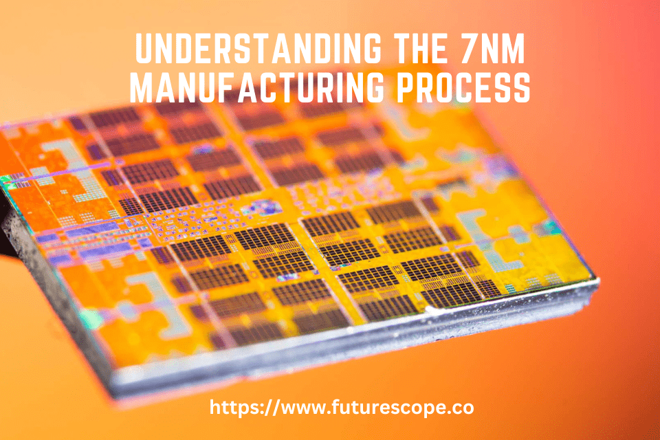
As technology advances, so does the need for smaller, faster, and more efficient devices. One of the key components in achieving this is the manufacturing process of the electronic chips that power these devices. The 7nm manufacturing process is a recent breakthrough in the semiconductor industry that has allowed for the creation of smaller and more powerful chips than ever before.
At its core, the 7nm manufacturing process refers to the size of the transistors that make up the electronic chips. The smaller the transistors, the more can be packed into a single chip, resulting in faster and more energy-efficient devices. The 7nm process is currently the most advanced commercially available process, with some companies already pushing the boundaries with experimental 5nm and 3nm processes.
The 7nm process has been a game-changer in the industry, allowing for the creation of powerful CPUs, GPUs, and other chips that have revolutionized the way we use technology. With its ability to pack more transistors into a smaller space, the 7nm process has enabled the creation of smaller and more powerful devices, from smartphones and tablets to data centers and supercomputers.
What is a Manufacturing Process?
When we talk about a manufacturing process, we’re referring to the series of steps that are involved in the creation of a product. This process includes the use of machinery, devices, and labor to convert raw materials into finished goods. Each step in the process is carefully designed to ensure that the final product meets the required quality standards, tolerances, and performance metrics.
Manufacturing processes can vary widely depending on the product being created. For example, the process used to manufacture a car is very different from the process used to create a smartphone. However, there are some commonalities between all manufacturing processes, such as the need for raw materials, quality control, and testing.
One of the key goals of any manufacturing process is to minimize waste and increase efficiency. This can be achieved through the use of automation, lean manufacturing techniques, and other process improvements. By optimizing the manufacturing process, companies can reduce costs, improve product quality, and increase their competitiveness in the marketplace.
What is Nanometer?
In the world of electronics, nanometer is a term used to describe the size of transistors and other components used in the manufacturing of electronic devices. A nanometer is one billionth of a meter, which means it is incredibly small. To put it into perspective, a human hair is about 100,000 nanometers thick.
The size of these components is important because it affects the power efficiency and performance of electronic devices. Smaller components mean less power is required to perform the same tasks, which results in more energy-efficient devices. Additionally, smaller components allow for more components to be packed into the same physical space, resulting in more powerful and capable devices.
As technology advances and manufacturers are able to create even smaller components, we can expect to see even more powerful and energy-efficient electronic devices in the future.
What is 7nm Manufacturing Process?
7nm manufacturing process is the latest technology node in the semiconductor industry. It is a significant milestone that has revolutionized the way we design and manufacture computer chips. The term “7nm” refers to the size of the transistor gates that are etched onto the silicon wafer. In other words, the distance between the source and drain of a transistor is only 7 nanometers, which is incredibly small.
With the 7nm manufacturing process, chip manufacturers can pack more transistors onto a single chip, which means more computing power, better performance, and lower power consumption. The 7nm process has enabled the development of smaller, faster, and more efficient chips for a wide range of applications, including mobile devices, artificial intelligence, cloud computing, and more.
At the heart of the 7nm manufacturing process is FinFET technology, which stands for Fin Field-Effect Transistor. FinFET is a type of multi-gate transistor that allows for better control of the flow of electrons, resulting in faster and more efficient performance. The 7nm process also uses extreme ultraviolet (EUV) lithography, which allows for more precise and accurate patterning of the silicon wafer.
The 7nm manufacturing process is not without its challenges, however. As the transistor gates become smaller, it becomes harder to control the flow of electrons, which can result in leakage and other issues. Additionally, the cost of developing and manufacturing chips using the 7nm process is higher than previous generations, which has led to consolidation in the industry.
Why is 7nm Manufacturing Process Important?
The 7nm manufacturing process is important for several reasons, including:
Improved Performance: With the 7nm process, we can expect to see a significant improvement in performance. This is because the smaller transistors allow for more transistors to be packed onto a single chip, resulting in faster processing speeds and more efficient power consumption.
Reduced Power Consumption: One of the biggest advantages of the 7nm process is its ability to reduce power consumption. With smaller transistors, less power is required to switch them on and off, resulting in less heat generated and longer battery life for mobile devices.
Increased Density: The 7nm process allows for a higher transistor density, which means more transistors can be placed on a single chip. This allows for more complex and powerful processors to be built, which is important for applications such as artificial intelligence, machine learning, and high-performance computing.
Cost Savings: While the 7nm process is more expensive than previous processes, it can ultimately lead to cost savings for manufacturers. This is because the smaller transistors allow for more chips to be produced on a single wafer, reducing manufacturing costs per chip.
In summary, the 7nm manufacturing process is important because it offers improved performance, reduced power consumption, increased density, and cost savings. As technology continues to advance, we can expect to see even smaller and more advanced manufacturing processes in the future.
How is 7nm manufacturing process achieved?
7nm manufacturing process is achieved through a combination of various patterning technologies, including pitch splitting, self-aligned patterning, and EUV lithography. These technologies carry significant challenges in critical dimension (CD) control as well as pattern placement, all involving neighboring features.
The 7nm process features SAQP for the FEOL, and double patterning for the BEOL. GlobalFoundries claims a 2.8 times density improvement compared to their 14nm process, and a performance improvement of 40% or a 55% reduction in power consumption. Two versions of the process will be developed: a low power version for mobile applications.
One of the key components of the 7nm manufacturing process is the use of Fin Field-Effect Transistor (FinFET) technology. TSMC’s 7nm FinFET process technology sets the industry pace for 7nm process technology development by delivering 256Mb SRAM with double-digit yields in June 2016. In 2019, in N7 process node’s second year of volume production, customers taped out more than 110 new generation products on N7.
Intel’s 7nm development is progressing well, driven by increased use of extreme ultraviolet lithography (EUV) in a rearchitected, simplified process flow. Intel prepares to send its first 7nm CPU off for manufacturing. The company’s 7nm development is progressing well, driven by increased use of extreme ultraviolet lithography (EUV) in a rearchitected, simplified process flow.
Applications of 7nm Manufacturing Process
The 7nm manufacturing process is a significant improvement over its predecessor, the 10nm process, and has enabled the development of smaller, faster, and more power-efficient chips. This has led to a wide range of applications across various industries. In this section, we will discuss some of the most prominent applications of the 7nm manufacturing process.
1. Mobile Devices: The 7nm process has been widely adopted in the mobile device industry due to its ability to produce smaller, more power-efficient chips. This has enabled the development of more advanced smartphones and tablets with longer battery life and better performance. For example, the Apple A12 Bionic chip used in the iPhone XS and XR is manufactured using the 7nm process and has significantly improved performance and power efficiency compared to its predecessor.
2. Artificial Intelligence: The 7nm process has also been instrumental in the development of artificial intelligence (AI) applications. The smaller, more power-efficient chips produced by this process are ideal for running complex AI algorithms, which require a significant amount of computing power. This has led to the development of more advanced AI-enabled devices such as smart speakers, autonomous vehicles, and robotics.
3. High-Performance Computing: The 7nm process has also enabled the development of high-performance computing (HPC) applications. The smaller, more power-efficient chips produced by this process are ideal for running complex simulations and calculations. This has led to the development of more advanced HPC systems used in scientific research, weather forecasting, and financial modeling.
4. Graphics Processing: The 7nm process has also been widely adopted in the graphics processing industry. The smaller, more power-efficient chips produced by this process are ideal for running advanced graphics-intensive applications such as video games and virtual reality. For example, the AMD Radeon VII graphics card is manufactured using the 7nm process and offers significantly improved performance and power efficiency compared to its predecessor.
Overall, the 7nm manufacturing process has enabled the development of smaller, faster, and more power-efficient chips, which have found applications across various industries. As the demand for more advanced and complex devices continues to grow, the 7nm process is expected to play an increasingly important role in shaping the future of technology.
Challenges in 7nm Manufacturing Process
As we move towards the 7nm manufacturing process, several challenges need to be addressed to ensure smooth production and yield high-quality chips. Some of the significant challenges we may face are:
1. Critical Dimension Control: The 7nm foundry node is expected to utilize various patterning technologies, including pitch splitting, self-aligned patterning, and EUV lithography. Each of these technologies carries significant challenges in critical dimension (CD) control as well as pattern placement, all involving neighboring features. Achieving precise control over the critical dimensions is crucial to ensure that the chip operates efficiently and reliably.
2. Leakage: As the transistor dimensions shrink, the leakage current increases, leading to higher power consumption and reduced battery life. Leakage is a significant concern in 7nm manufacturing, and chip designers need to ensure that their designs minimize leakage and power consumption.
3. Unstable Parasitic Structures: Parasitic structures are unwanted capacitive or resistive elements that can affect circuit performance. As we move towards smaller nodes, these parasitic structures become more challenging to control, leading to unstable circuit behavior. Designers need to account for these parasitic structures and ensure that their designs minimize their impact on circuit performance.
4. Defects and Imperfections: Defects and imperfections are inevitable in the manufacturing process, and as we move towards smaller nodes, these defects become more challenging to detect and correct. Defects can cause significant issues in circuit performance, and manufacturers need to ensure that their manufacturing processes are robust and minimize defects and imperfections.
5. Cost: The cost of manufacturing at the 7nm node is significantly higher than previous nodes due to the complexity of the manufacturing process and the need for advanced equipment. Manufacturers need to ensure that they can produce chips at a reasonable cost while maintaining high yields and quality.
Overall, the move towards the 7nm manufacturing process presents several challenges that need to be addressed to ensure smooth production and yield high-quality chips. By addressing these challenges, we can continue to push the limits of technology and bring new and innovative products to the market.
Future of 7nm Manufacturing Process
As we have seen, the 7nm manufacturing process has revolutionized the semiconductor industry, enabling the production of smaller, faster, and more power-efficient chips. However, the future of the 7nm process is uncertain, with some experts predicting that it may be the last node in Moore’s Law.
Moore’s Law, which states that the number of transistors on a chip doubles every two years, has been the driving force behind the semiconductor industry for decades. However, as the size of transistors approaches the atomic scale, it becomes increasingly difficult and expensive to manufacture them. This has led some experts to predict that the 7nm process may be the end of Moore’s Law.
However, others believe that there is still room for innovation and improvement in the 7nm process. For example, companies like Intel and TSMC are already working on new technologies such as EUV lithography and gate-all-around transistors, which could enable the production of even smaller chips.
Moreover, the demand for faster and more power-efficient chips is only increasing, driven by emerging technologies such as 5G, AI, and IoT. This means that there will continue to be a need for smaller and more advanced chips, which could drive further innovation in the 7nm process.
Overall, the future of the 7nm manufacturing process is uncertain, but there is still potential for further innovation and improvement. As technology continues to advance, we can expect to see new and exciting developments in the semiconductor industry, driven by the demand for faster, more powerful, and more efficient chips.