
What We Have Covered in This Article
Last Updated on April 14, 2023 by Editor Futurescope
Semiconductor chips are essential components in modern electronics, from smartphones to cars. However, the process of making these chips is incredibly complex and time-consuming. It takes years to build semiconductor fabrication facilities, and even then, the economics are so brutal that companies can lose out if their products do not sell well.
The global chip shortage has highlighted just how difficult it is to make semiconductors. The shortage has impacted various industries, including automobiles, appliances, and even video game consoles. The shortage is due to a combination of factors, including the COVID-19 pandemic, increased demand for electronics, and supply chain disruptions.
Manufacturing semiconductor chips requires a skilled workforce and specialized equipment. The process involves hundreds of steps and can take months from design to production. The most crucial and expensive pieces of equipment in a chip factory run about 90% of the time, with 10% downtime for scheduled or urgent maintenance.
Overview of the Semiconductor Manufacturing Process
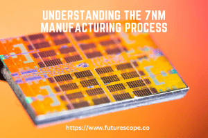
The process of semiconductor manufacturing is a complex and highly precise process that involves a series of steps to create tiny electronic components that are used in a variety of devices. The process starts with the creation of a silicon wafer, which is then processed to create the individual components.
The manufacturing process involves several stages, including design, fabrication, packaging, and testing. The design stage involves creating a blueprint for the chip using computer-aided design (CAD) software. The fabrication stage involves creating the chip on a silicon wafer using a series of photolithography and etching processes. This process involves layering the wafer with various materials and then etching away portions of the material to create the desired pattern.
After the fabrication stage, the chips are cut from the wafer and undergo a packaging process. This involves encapsulating the chip in a protective casing and connecting it to a substrate. The final stage in the process is testing, which involves checking the functionality of the chip to ensure that it meets the required specifications.
The semiconductor manufacturing process is highly complex and requires a high degree of precision and attention to detail. It involves a large number of steps, each of which must be carefully controlled to ensure that the final product is of high quality. The process also requires a significant investment in equipment and facilities, as well as highly skilled personnel to operate and maintain the equipment.
Designing the Chip
Designing a semiconductor chip is a complex and expensive process that requires cutting-edge technology and significant investment. According to a report by McKinsey & Company, designing a 5 nm chip costs about $540 million for everything from validation to IP qualification. This is well above the $175 million required to design a 10 nm chip and the $300 million required for a 7 nm chip. As technology advances and the demand for more powerful chips increases, R&D costs are expected to continue to escalate, especially for leading-edge products.
Designing a chip involves several steps, including:
- Defining the chip’s functionality and specifications
- Designing the chip’s architecture and circuitry
- Verifying the chip’s functionality and performance
- Testing the chip’s reliability and durability
Each step requires specialized software tools, such as computer-aided design (CAD) software and simulation tools, to ensure the chip meets the required specifications and performance standards. The design process also involves working with semiconductor foundries to ensure the chip can be manufactured using the latest technology and processes.
One of the biggest challenges in designing a semiconductor chip is ensuring that it can be manufactured at scale with high yields. This requires careful consideration of factors such as the chip’s size, complexity, and power consumption, as well as the manufacturing process itself. Designers must also consider the cost of manufacturing the chip, which can be significant, especially for leading-edge products.
Despite the challenges, semiconductor companies continue to invest heavily in chip design and R&D to meet the growing demand for more powerful and efficient chips. As technology advances and new applications emerge, the demand for semiconductor chips is expected to continue to grow, making chip design and manufacturing a critical part of the global economy.
Masking and Lithography
One of the most crucial steps in semiconductor manufacturing is lithography. Lithography is the process of transferring a pattern from a photomask to a substrate, which is typically a silicon wafer. This process is essential because it determines how small the transistors on a chip can be. During this stage, the chip wafer is inserted into a lithography machine, where it’s exposed to deep ultraviolet (DUV) or extreme ultraviolet (EUV) light. The light has a wavelength anywhere from 365 nm for less complex chip designs to 13.5 nm for more advanced chips.
A lithography system is essentially a projection system. Light is projected through a blueprint of the pattern that will be printed, known as a mask or reticle. With the pattern encoded in the light, the system’s optics shrink and focus the pattern onto the photosensitive silicon wafer. The mask is a critical component of the lithography process because it determines the pattern that will be printed on the substrate. The mask is typically made of quartz or glass and is etched with the desired pattern using a process called photomask fabrication.
The photomask fabrication process involves using an attenuated phase-shifting background film on the mask to increase the contrast of small intensity peaks, or etching the exposed quartz so that the edge between the etched and unetched areas can be used to image nearly zero intensity. The mask is then inspected and cleaned to ensure that it’s free of defects that could negatively impact the final chip’s performance. The mask is then loaded into the lithography machine, and the chip manufacturing process continues.
Etching and Deposition
Etching and deposition are two important processes in semiconductor chip manufacturing. Etching removes unwanted material from the surface of the wafer, while deposition adds new material to the surface. These processes are used to create the intricate patterns and structures that make up a semiconductor chip.
Etching is typically done using a chemical solution or plasma. The solution selectively removes material from the wafer surface, leaving behind the desired pattern. Plasma etching uses a high-energy plasma to remove material, which can be more precise and controlled than chemical etching.
Deposition involves adding a thin layer of material to the wafer surface. This can be done using techniques such as chemical vapor deposition (CVD) or physical vapor deposition (PVD). CVD involves introducing a gas into a chamber and allowing it to react and deposit onto the wafer surface. PVD uses a vacuum to evaporate a material and deposit it onto the wafer surface.
Both etching and deposition require careful control and monitoring to ensure that the desired patterns and structures are created. Any errors or defects in these processes can lead to faulty chips or reduced yields, which can be costly for manufacturers.
Testing and Packaging
Once the semiconductor chip has been manufactured, it needs to be tested and packaged before it can be used in electronic devices. Testing is a crucial step to ensure that the chip meets the required specifications and functions properly. There are several types of tests that are performed, including:
- Functional testing: This test checks if the chip performs its intended function correctly.
- Parametric testing: This test measures the chip’s electrical characteristics, such as voltage and current, to ensure that they meet the required specifications.
- Reliability testing: This test checks if the chip can withstand various environmental conditions, such as temperature and humidity, over a period of time.
After testing, the chip is packaged. Packaging is the process of encapsulating the chip in a protective material and connecting it to the outside world through metal leads. Packaging serves several purposes, including:
- Protecting the chip from mechanical and environmental damage
- Providing electrical connections to the chip
- Dissipating heat generated by the chip
There are several types of packaging, including:
- Through-hole packaging: This is an older type of packaging where the leads of the chip are inserted into holes in a printed circuit board (PCB) and soldered in place.
- Surface-mount packaging: This is a newer type of packaging where the chip is mounted on the surface of the PCB and connected to it using metal pads and solder.
- Ball grid array (BGA) packaging: This is a type of surface-mount packaging where the chip is mounted on a small substrate that has metal balls on its underside. The balls are used to make electrical connections to the PCB.
Challenges in Semiconductor Manufacturing
Semiconductor manufacturing is a complex process that involves multiple stages, each with its own set of challenges. Here are some of the key challenges in semiconductor manufacturing:
1. High Capital Costs: Building a semiconductor fabrication facility, commonly known as a fab, is a capital-intensive process that requires a significant upfront investment. According to McKinsey, the cost of building a new fab can range from $3 billion to $10 billion, depending on the technology and capacity required. This high capital cost makes it challenging for new entrants to enter the market and compete with established players.
2. Complexity of the Manufacturing Process: The manufacturing process for semiconductors is highly complex and involves multiple steps, including lithography, etching, deposition, and polishing. Each step requires specialized equipment and expertise, and any errors or defects in one step can impact the entire process, leading to yield loss and increased costs.
3. Shortage of Skilled Workers: The semiconductor industry is facing a shortage of skilled workers, particularly in areas such as process engineering and equipment maintenance. This shortage is partly due to the high demand for skilled workers in other industries, such as software development and data science.
4. Supply Chain Disruptions: The semiconductor industry relies on a complex global supply chain, with many components and materials sourced from different countries. Any disruptions in the supply chain, such as natural disasters, trade disputes, or pandemics, can lead to shortages and price increases.
. Environmental Concerns: Semiconductor manufacturing involves the use of hazardous chemicals and generates a significant amount of waste. As a result, the industry is under increasing pressure to adopt more sustainable practices and reduce its environmental footprint. In summary, semiconductor manufacturing is a highly complex and capital-intensive process that faces multiple challenges, including high costs, process complexity, shortage of skilled workers, supply chain disruptions, and environmental concerns. Addressing these challenges will be critical to ensuring the continued growth and innovation of the semiconductor industry.
Future of Semiconductor Technology
The future of semiconductor technology is promising, as new advancements are being made to address the challenges faced by the industry. One such advancement is the use of multi-die systems, which allow for the integration of multiple chips onto a single package. This approach offers several benefits, including improved performance, reduced power consumption, and increased flexibility.
Another area of focus is the development of alternative materials for chip manufacturing. Silicon has been the go-to material for decades, but its limitations are becoming increasingly apparent as chip sizes continue to shrink. Researchers are exploring new materials such as gallium nitride and silicon carbide, which offer superior performance and efficiency compared to silicon.
Furthermore, the industry is investing heavily in research and development to improve the manufacturing process. The US government has committed $52 billion to semiconductor manufacturing and research, with a significant portion allocated to subsidizing the building of factories domestically. This investment is critical to ensuring that the US remains competitive in the global market.
Overall, the future of semiconductor technology is exciting, with new advancements and innovations on the horizon. As the industry continues to evolve, it will be interesting to see how these developments shape the future of computing and technology.